Printed Circuit Boards (PCBs) are the silent backbone of nearly every electronic device we use today. From smartphones to solar inverters, a well-designed PCB ensures reliability and performance. In our Shenzhen facility, we’ve noticed that even small design choices—like choosing a 1.6mm board thickness or the right copper weight—can make a big difference in signal integrity and durability.
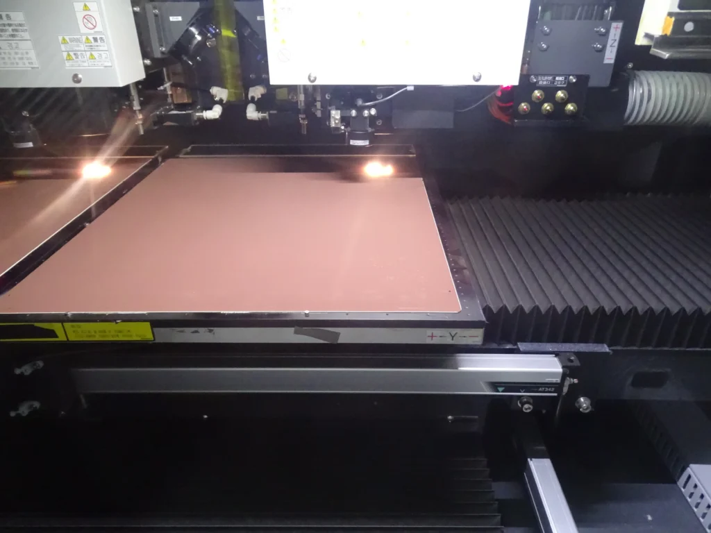
The PCB manufacturing process starts with detailed layout design. Engineers carefully translate schematics into board layers, considering trace width, via placement, and impedance requirements. Once the design is finalized, we select high-quality materials such as FR-4 or advanced laminates, followed by copper layering, etching, and precision drilling. Each step is monitored with automated machinery and visual inspections to maintain tight tolerances and minimize defects.
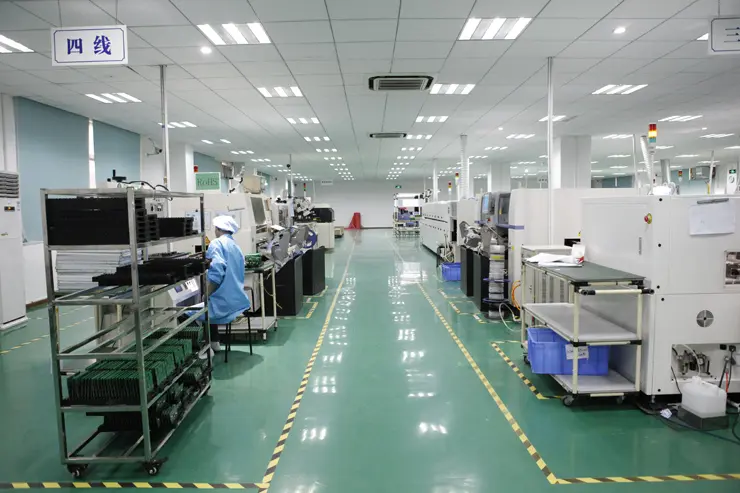
After fabrication, the boards move to assembly. Components—ranging from tiny 0402 resistors to large ICs—are mounted using Surface Mount Technology (SMT) or Through-Hole Technology (THT), depending on the project. We perform 100% electrical testing and functional inspections to ensure every board meets client specifications. These quality checks prevent issues in mass production and save customers time and cost.
Understanding the PCB process helps engineers and product developers make better design and sourcing decisions. Partnering with experienced PCB manufacturers, who understand local supply chains and production nuances, is crucial for fast prototyping and reliable mass production. At the end of the day, a carefully crafted PCB isn’t just a board—it’s the heart of every electronic device.