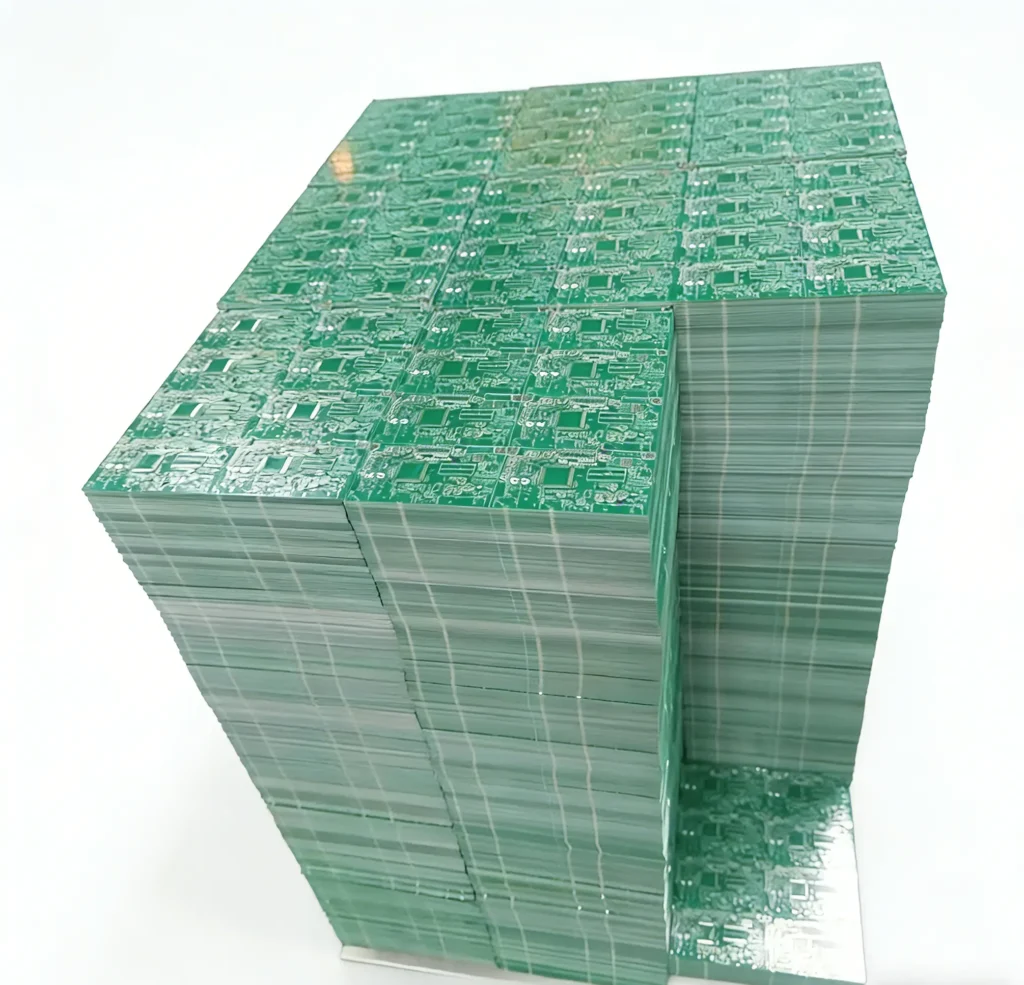
Printed circuit boards (PCBs) are the backbone of nearly every electronic product, from smartphones and industrial equipment to home appliances. While engineers and buyers often focus on the finished PCB, understanding how a PCB is manufactured provides valuable insight into cost control, design optimization, and supplier selection.
In this article, we provide a detailed walkthrough of the PCB manufacturing process, using a standard double-sided PCB as an example. This step-by-step guide explains how raw materials are transformed into ready-to-use circuit boards and why each stage matters.
Overview of the PCB Manufacturing Process
The PCB fabrication process is not a single operation but a carefully controlled sequence of steps. It can be divided into three main phases:
Pre-production preparation and engineering
Circuit pattern transfer and etching
Surface finishing, testing, and final inspection
Each phase plays a critical role in ensuring PCB quality, reliability, and long-term performance.
Phase 1: Pre-Production Preparation and Engineering
This phase converts PCB design data into manufacturing-ready production files.
Copper-Clad Laminate (CCL): The Base Material
PCB manufacturing starts with copper-clad laminate (CCL), which consists of thin copper foil bonded to an insulating substrate, most commonly FR-4 fiberglass.
The quality of the CCL directly affects signal integrity, mechanical strength, and overall PCB reliability.
PCB Design Review and CAM Processing
After receiving Gerber files, PCB manufacturers perform CAM (Computer-Aided Manufacturing) processing to verify manufacturability. Key checks include:
Trace width and spacing compliance
Hole size accuracy and tolerances
Panelization layout for efficient mass production
Early design review helps prevent production defects and reduces manufacturing cost.
Phototool (Film) Creation
Once the design is finalized, the data is transferred to phototools (films).
These films function like large photographic negatives and are used later during the PCB image transfer process.
Phase 2: Circuit Pattern Transfer and Etching
This is the core stage of the PCB fabrication process, where the electrical circuits are physically formed.
Drilling and Hole Metallization
Drilling: Precision drilling creates component holes and vias
Hole metallization (PTH): Copper is deposited on hole walls to electrically connect both sides of the board
This step is essential for double-sided PCB manufacturing and all multilayer PCBs.
Image Transfer Using Photolithography
Most PCBs use photolithography to achieve high circuit accuracy.
Photoresist coating
A light-sensitive photoresist (dry film or liquid) is applied evenly to the copper surface.UV exposure
The phototool is aligned and exposed under ultraviolet light. Exposed areas harden, while unexposed areas remain soluble.Developing
A developer solution removes the unexposed photoresist, leaving the circuit pattern protected on the copper.
PCB Etching Process
The board passes through an etching machine using acidic or alkaline solutions (such as cupric chloride):
Unprotected copper is etched away
Protected copper traces remain intact
This step defines the final PCB circuit layout.
Stripping (Photoresist Removal)
After etching, the remaining photoresist is chemically stripped, exposing clean copper traces ready for further processing.
Phase 3: Surface Finishing, Testing, and Quality Control
This phase protects the PCB, improves solderability, and ensures product quality.
Solder Mask Application
A solder mask—most commonly green, but also available in red, blue, black, or white—is applied to:
Protect copper traces from oxidation
Prevent solder bridging during PCB assembly
Silkscreen Printing
Silkscreen printing adds component reference designators, symbols, and logos on the PCB surface, improving assembly accuracy and traceability.
PCB Surface Finish
To prevent oxidation and ensure good solderability, a surface finish is applied. Common PCB surface finish types include:
HASL (Hot Air Solder Leveling)
ENIG (Electroless Nickel Immersion Gold)
Immersion Tin
Immersion Silver
OSP (Organic Solderability Preservative)
Profiling and Routing
The PCB panel is separated into individual boards using CNC routing or V-cut depaneling, depending on the design requirements.
Electrical Testing
Electrical testing checks for:
Open circuits
Short circuits
Netlist accuracy
This step ensures that every PCB meets electrical performance specifications.
Final Inspection and Packaging
After visual inspection and dimensional checks, qualified PCBs are carefully packaged to prevent damage during transportation.
Additional Process for Multilayer PCB Manufacturing
For multilayer PCB manufacturing, an additional lamination step is required.
Inner-layer boards, prepreg sheets, and outer copper foils are stacked and bonded together under high temperature and pressure to form a single, solid PCB structure.
Summary: PCB Manufacturing Process Step by Step
Material cutting → Drilling → Hole metallization → Image transfer → Etching → Stripping →
Solder mask → Silkscreen → Surface finish → Profiling → Electrical testing → Final inspection → Packaging
Why Understanding the PCB Manufacturing Process Matters
A clear understanding of the PCB production process helps you:
Design boards optimized for manufacturability (DFM)
Reduce production cost and lead time
Communicate more effectively with PCB manufacturers
Whether you are sourcing custom PCBs, double-sided PCBs, or multilayer PCBs, knowing how PCBs are made is a strong advantage when selecting the right supplier.
