Engineering-Driven Rigid Flex Circuit Board Fabrication
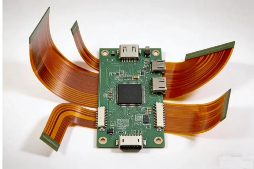
Rigid-Flex PCBs are not simply a combination of a rigid PCB and a flexible PCB.
They are highly integrated circuit boards that place strict requirements on material selection, stack-up design, process control, and long-term reliability.
In our factory, Rigid-Flex PCB manufacturing starts from engineering review, not from material loading.
This engineering-first approach ensures stable mass production, high yield, and reliable performance in real applications.
1. Engineering Review & Stack-Up Validation
(Critical Front-End Process for Rigid-Flex PCB Manufacturing)
Before production begins, our engineering team conducts a comprehensive DFM and DFA review, focusing on:
Rationality of rigid and flex area partitioning
Bend locations, bend radius, and compatibility with stack-up design
Selection of coverlay, stiffeners, and lamination sequence
Manufacturability of laser-drilled vias and mechanically drilled holes
Potential stress concentration and long-term reliability risks
The goal at this stage is not whether the rigid-flex PCB can be made, but whether it can be produced consistently with controlled yield and reliability.
Keywords embedded: rigid-flex PCB engineering review, rigid flex stack-up design, DFM for rigid-flex PCB
2. Material Preparation & Precision Cutting
Based on the confirmed structure, rigid and flexible materials are managed and processed separately:
Rigid area: High-Tg FR-4 or specified high-reliability copper clad laminates
Flexible area: Polyimide (PI) base material, adhesive films, coverlay, and PI stiffeners
All materials are precisely cut according to engineering dimensions, with strict control over material batch, thickness tolerance, and grain direction, ensuring a stable foundation for lamination and bonding.
Keywords embedded: rigid-flex PCB materials, PI flexible circuit material, high Tg FR-4 rigid flex
3. Independent Fabrication of Rigid and Flexible Circuits
Before combining rigid and flexible sections, circuit fabrication is completed independently:
Rigid sections: Inner and outer layer imaging, etching, and layer alignment
Flexible sections: Fine-line circuit fabrication with tight control of trace width, spacing, and copper thickness uniformity
This separation ensures high circuit accuracy, consistency, and yield, especially for high-density rigid-flex PCB designs.
Keywords embedded: rigid flex PCB circuit fabrication, fine line flexible PCB, HDI rigid flex PCB
4. Lay-Up and Multi-Step Lamination Control
(Core Capability of Rigid-Flex PCB Manufacturing)
Rigid-Flex PCBs typically require multiple lamination cycles and staged pressing processes, including:
Accurate material lay-up between rigid and flexible layers
Precise control of resin flow, pressure profiles, and temperature curves
Prevention of adhesive overflow in flex areas and voids or misregistration in rigid areas
This process directly determines the mechanical stability, interlayer bonding strength, and long-term reliability of the rigid-flex circuit board—and is a key indicator of a manufacturer’s technical capability.
Keywords embedded: rigid flex PCB lamination, multi-step lamination rigid flex, rigid flex PCB reliability
5. Drilling Process: Laser Drilling & Mechanical Drilling
Depending on the product structure, we apply a hybrid drilling strategy:
Laser drilling: Microvias and high-density interconnections, especially in flexible areas
Mechanical drilling: Through holes and structural holes in rigid sections
Special attention is paid to hole accuracy and hole wall quality in rigid-flex transition zones, minimizing risks caused by material differences.
Keywords embedded: laser drilling rigid flex PCB, microvia rigid flex, rigid flex drilling process
6. Hole Metallization & Copper Plating
After drilling, the boards undergo:
Electroless copper deposition
Electrolytic copper plating
This ensures continuous, uniform copper coverage on hole walls, providing reliable electrical interconnection across multiple layers.
Keywords embedded: rigid flex PCB plating, via metallization rigid flex, through hole copper plating PCB
7. Circuit Patterning, Solder Mask & Coverlay Application
Rigid areas: Solder mask application with precise pad opening control
Flexible areas: Coverlay lamination to enhance bend durability and fatigue resistance
For rigid-flex PCBs, we place particular emphasis on flex area flexibility, bend life, and resistance to repeated mechanical stress.
Keywords embedded: rigid flex solder mask, rigid flex coverlay, flexible PCB bend reliability
8. Routing, Electrical Testing & Reliability Validation
Precision routing to ensure accurate rigid-flex boundary dimensions
Flying probe or electrical testing to verify circuit continuity and functionality
Optional reliability tests such as bending tests, thermal cycling, and environmental stress testing
Our objective is to ensure that every rigid-flex PCB is not only electrically qualified, but also reliable throughout its service life.
Keywords embedded: rigid flex PCB testing, flying probe test rigid flex, rigid flex reliability testing
Conclusion: Engineering-Driven Rigid-Flex PCB Manufacturing
In our factory, Rigid-Flex PCB manufacturing is not a standardized assembly-line process, but a system-level engineering solution focused on reliability and mass-production stability.
We prioritize:
Suitability for volume production
Long-term electrical and mechanical reliability
Real alignment with the customer’s application requirements
This is how we deliver high-quality, reliable rigid-flex PCB solutions for demanding applications.