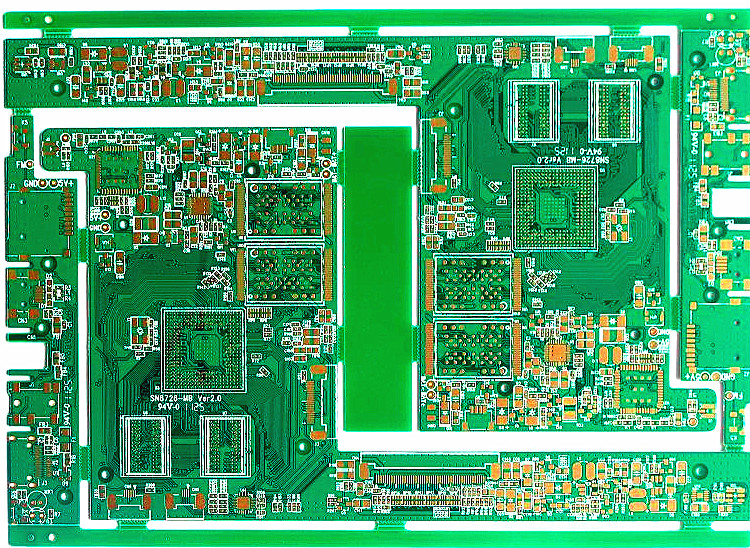
When engineers or buyers search for hdipcbcost, they are usually comparing HDI boards against conventional multilayer PCBs and asking one direct question:
Why is the price difference so large — often two to four times higher?
The answer is not marketing or supplier margins.
HDI PCB cost is driven by non-negotiable manufacturing constraints.
This article explains, with quantitative production data, why HDI PCBs are structurally more expensive and what actually determines hdipcbcost.
1. HDI PCB Cost Is Density-Driven, Not Layer-Driven
A common assumption is that HDI cost depends mainly on layer count.
In reality, interconnect density is the dominant cost driver.
Typical cost impact by design rules:
-
Line width / spacing ≥ 100/100 μm → baseline cost
-
Line width / spacing 75/75 μm → +20–30%
-
Line width / spacing 50/50 μm → +45–70%
-
Microvia diameter ≤ 100 μm → +25%
-
Stacked microvias → +35–50%
Conclusion:
An 8-layer HDI PCB with microvias costs 1.8–2.5× more than a conventional 8-layer PCB of the same size.
This rule defines hdipcbcost and cannot be bypassed.
2. Material Grade Raises hdipcbcost by 30–80%
HDI PCBs require dimensionally stable laminates with controlled Z-axis expansion.
Material cost comparison:
-
Standard FR-4 (Tg 135): 1.0×
-
High Tg FR-4 (Tg ≥ 170): 1.2–1.4×
-
HDI-grade FR-4 (low CTE): 1.5–1.8×
-
Polyimide (PI): 2.5–3.5×
-
PTFE-based laminate: 3.0–5.0×
In production, materials account for 35–45% of total hdipcbcost, compared to 20–25% in standard PCBs.
Low-grade laminates fail HDI reliability testing and are not viable alternatives.
3. Laser Drilling Is a Fixed Cost Component
HDI PCBs rely on laser-drilled microvias, not mechanical drilling.
Production facts:
-
Microvias per HDI panel: 80,000–200,000
-
Laser drilling speed: 80,000–120,000 vias/hour
-
Laser drilling contribution: 15–25% of hdipcbcost
Each additional build-up layer requires a complete repetition of laser drilling and plating.
Stacked microvias always cost more than staggered microvias — without exception.
4. Multiple Plating Cycles Multiply Cost Linearly
HDI boards undergo multiple independent copper plating cycles.
For a typical 2+N+2 HDI structure:
-
3–4 copper plating cycles
-
Via filling (resin or copper)
-
Surface planarization
Cost impact:
-
Resin-filled microvias: +10–15%
-
Copper-filled microvias: +20–30%
-
Any-layer HDI structure: +40–60%
Plating-related steps alone contribute up to 30% of total hdipcbcost.
 Why hdipcbcost Varies So Much Between Suppliers
Many HDI PCB quotations differ not because of material prices, but due to process control, yield management, and inspection standards.
We quote HDI PCBs based on:
-
Proven HDI yield data, not theoretical capacity
-
Actual laser drilling and plating cycles
-
Mandatory X-ray and impedance testing
This is why two HDI quotes with identical specifications can differ by more than 40%.
If you are comparing hdipcbcost between suppliers, request a technology-based quotation, not a price-only offer.
5. Yield Loss Is the Silent Cost Driver
HDI PCB yield is structurally lower than conventional PCB yield.
Typical production yield:
-
Standard multilayer PCB: 92–96%
-
Sequential HDI PCB: 75–85%
-
Any-layer HDI PCB: 65–75%
Every 1% reduction in yield increases hdipcbcost by 1.3–1.6%.
This is why stable HDI manufacturers do not compete on extreme low pricing.
6. Testing and Inspection Add 12–18% to hdipcbcost
HDI PCBs require mandatory inspection steps:
-
AOI at every build-up layer
-
X-ray inspection for blind and buried vias
-
Electrical testing with reduced access
-
Controlled impedance verification (±10% or tighter)
Cost impact:
-
Standard PCB testing: +5–8%
-
HDI PCB testing: +12–18%
Skipping these steps does not save money — it causes field failure.
7. Realistic hdipcbcost Reference (Small–Mid Volume)
| HDI Structure | Cost vs Standard PCB |
|---|---|
| 1+N+1 HDI | 1.4–1.8× |
| 2+N+2 HDI | 1.8–2.5× |
| Any-layer HDI | 2.5–4.0× |
Assumptions:
-
Board size ≤ 100 × 100 mm
-
Volume: 1,000–10,000 pcs
-
Surface finish: ENIG
 Evaluate hdipcbcost Based on Your Actual Design
If you are evaluating hdipcbcost for an actual project, generic price ranges are not enough.
HDI PCB pricing depends on exact design rules, stack-up, via structure, and volume.
For boards of identical size, pricing differences of 30–50% are common due to design choices alone.
If you want an accurate HDI PCB quotation based on real manufacturing data, you can send us your Gerber files or stack-up requirements.
We provide:
-
Design-for-manufacturing feedback before pricing
-
Clear cost explanation for HDI structures
-
Stable mass production capability up to 16 layers
Requesting a quote early often reduces hdipcbcost before layout is finalized.
Final Takeaway
hdipcbcost is determined by physics and process limits, not negotiation.
Cost reduction is only achievable through:
-
Design-for-manufacturing optimization
-
Microvia count reduction
-
Build-up layer minimization
If HDI PCB pricing approaches standard PCB levels, reliability has already been compromised.
 Request an HDI PCB Quote
Need a reliable reference for hdipcbcost on your next HDI project?
Send us your Gerber files, stack-up details, or target quantity.
Our engineering team will review feasibility first and then provide a manufacturable, data-based quotation.
