Why HDI PCBs Cost More Than Standard PCBs
4 Key Factors That Drive the Price Difference
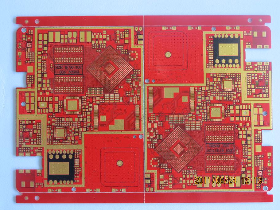
Many customers are surprised when they receive a quotation for an HDI (High Density Interconnect) PCB and find that the price is significantly higher than that of a standard PCB.
In reality, this price difference is not arbitrary. HDI PCBs require different materials, more advanced processes, longer production cycles, and stricter quality control. Below, we explain the four main reasons why HDI PCBs typically cost much more than conventional PCBs.
1. Higher Material Requirements
HDI PCBs place much stricter demands on base materials and copper foil compared to standard PCBs.
Thinner and More Specialized Laminates
Standard PCBs commonly use conventional FR-4 laminates with a thickness of around 1.6 mm.
HDI PCBs, however, often require:
-
Thin FR-4 laminates (typically 0.2–0.4 mm), or
-
High-speed / high-frequency materials such as PTFE for signal integrity requirements
Thin laminates are more difficult to process, while high-speed materials are significantly more expensive. As a result, material costs alone for HDI PCBs are usually 30–50% higher than for standard PCBs.
Finer Copper Foil
HDI designs feature much finer traces and spaces (often 0.05–0.1 mm), which require high-ductility copper foil, typically 12 μm or thinner.
By comparison, standard PCBs commonly use 25 μm copper foil.
Finer copper foil improves reliability but comes at a cost — it is around 40% more expensive than standard copper foil.
2. More Complex Manufacturing Processes
The core manufacturing processes of HDI PCBs are fundamentally more complex than those of traditional PCBs.
Laser Drilling vs. Mechanical Drilling
Standard PCBs rely on mechanical drilling, which is fast and cost-effective.
HDI PCBs require UV laser drilling to create microvias:
-
Laser drilling equipment costs 5–10 times more than mechanical drilling machines
-
Drilling speed is slower
-
The cost per via can be 8–10 times higher than mechanical drilling
Sequential Lamination
Standard PCBs are typically laminated once, with all layers pressed together in a single cycle.
HDI PCBs use sequential lamination, where layers are built up step by step.
This means:
-
Multiple lamination cycles (often 3–4 times)
-
Repeated alignment, drilling, and inspection
-
Higher labor and equipment usage
Each additional lamination step significantly increases manufacturing cost.
3. Lower Production Efficiency and Longer Lead Time
HDI PCBs require more process steps and tighter controls, which directly affects production efficiency.
-
Standard PCBs:
-
15–20 process steps
-
Typical lead time: 7–10 days
-
-
HDI PCBs:
-
25–30 process steps
-
Typical lead time: 15–20 days
-
In addition, HDI PCBs demand extremely tight tolerances (often ±0.02 mm). Frequent inspections are required throughout production, increasing downtime and reducing throughput.
Lower efficiency means fewer boards can be produced within the same time frame — increasing the cost per unit.
4. Stricter Inspection and Lower Yield
Due to their high density and precision requirements, HDI PCBs are more sensitive to manufacturing variations.
-
Yield rates for HDI PCBs are often 10–20% lower than for standard PCBs
-
Any defects can lead to scrapped panels, and those losses must be absorbed into the cost of acceptable boards
Inspection costs are also higher:
-
HDI PCBs require high-resolution AOI systems
-
Advanced AOI equipment can cost 3–5 times more than standard systems
-
Inspection costs per board increase accordingly
Conclusion: HDI PCB Cost Is a Result of Total Manufacturing Complexity
HDI PCBs are more expensive not because of a single factor, but because materials, processes, production time, and yield risks all increase simultaneously.
In many projects, early design optimization can significantly reduce costs:
-
Avoid HDI structures when they are not strictly necessary
-
Use lower-order blind/buried vias whenever possible
-
Balance electrical performance with manufacturability (DFM)
Working closely with an experienced PCB manufacturer during the design stage is often the most effective way to control HDI PCB costs.
About Us
We are a China-based PCB and PCBA manufacturer providing one-stop PCB manufacturing, assembly, and sourcing services for global electronics companies. With extensive experience in HDI and multilayer PCB production, we help customers optimize designs for performance, manufacturability, and cost.
If you would like assistance reviewing your PCB design or reducing manufacturing cost, feel free to contact us.