When a new product uses an HDI PCB, jumping straight into mass production is one of the highest-risk decisions a team can make.
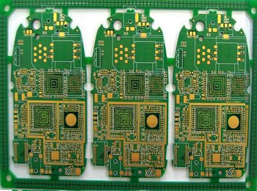
HDI boards are fundamentally different from standard multilayer PCBs. Laser-drilled microvias, multiple lamination cycles, tight registration tolerances, and copper reliability all introduce variables that don’t fully show up on drawings or simulations.
A small-batch HDI validation isn’t about slowing things down — it’s about turning unknown risks into known facts.
At the early stage of a new product, designs are rarely final. Stackups may still be optimized, via structures adjusted, and impedance or reliability margins fine-tuned. Questions like:
Is the microvia depth-to-diameter ratio truly manufacturable?
Can layer-to-layer alignment stay stable across production runs?
Does the structure deliver the expected yield, not just electrical performance?
These answers only come from real production, not theory.
A controlled small-batch HDI build allows teams to:
Confirm the design is suitable for mass production
Identify yield and reliability risks early
Optimize cost and delivery time before scaling
Many production failures don’t come from bad designs — they come from skipping the validation step.
For companies building products for the long term, a short validation phase often becomes the fastest and most cost-effective path to a successful launch.